Addressing 5 ROM Chips, Each of 4 KB Using 74LS138 Decoder:
The following diagram is representing the addressing of 5 ROM chips using 74LS138 where each chip is of 4 KB.
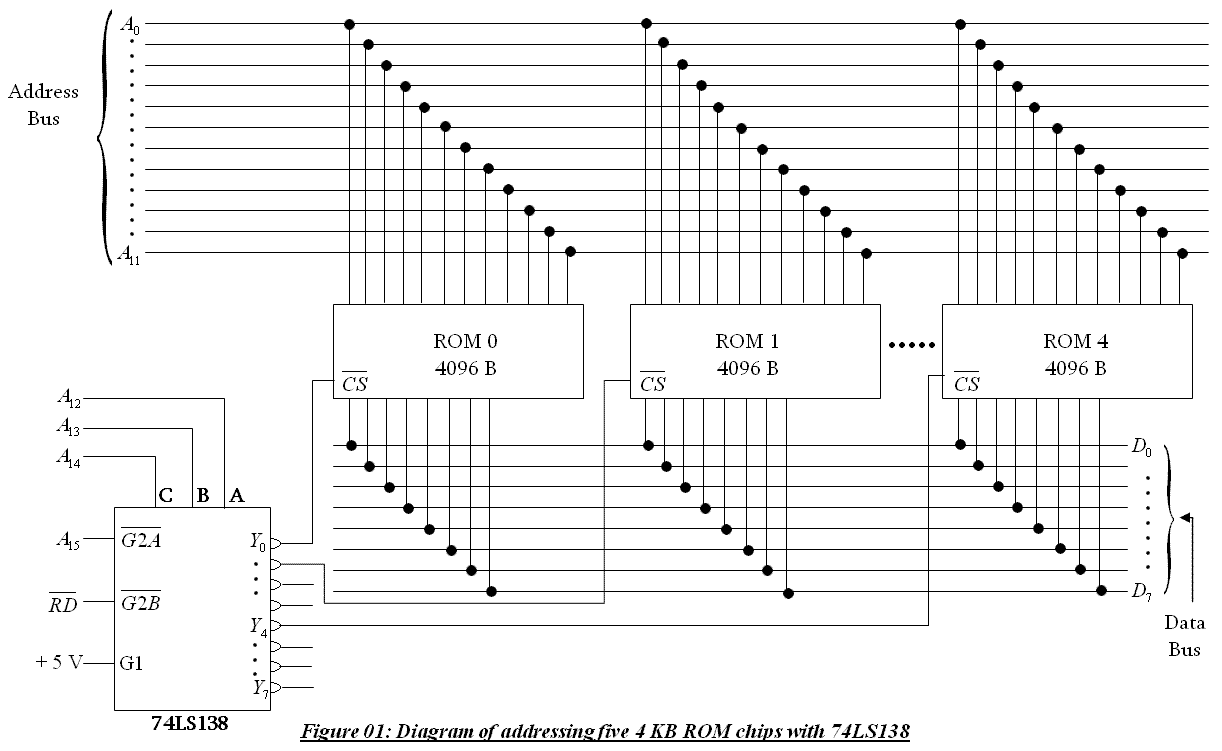
Explanation: From the previously given figure 01 it can be found that the Chip Select (CS) of the 5 ROM chips has been attached with the 74LS138. 8 data outputs of each chip have been connected to 8 data bus. As each ROM is of 4 KB or 212 B, each of them has been connected A12, A13, A14 to 12 address bus, from A0 to A11. 3-bits address A, B, C have been connected to respectively to get select inputs. Now, when the 74LS138 will be enabled by setting G2A & G2B to low and G1 to high, by the value of A, B, C a ROM will be selected to read. Now, how each location of each ROM will be selected can be determined by the following given worksheet or table;
|
215
A15
|
214
A14
|
213
A13
|
212
A12
|
211
A11
|
210
A10
|
29
A9
|
28
A8
|
27
A7
|
26
A6
|
25
A5
|
24
A4
|
23
A3
|
22
A2
|
21
A1
|
20
A0
|
||
|
ROM
0
|
Start
|
0
|
0
|
0
|
0
|
0
|
0
|
0
|
0
|
0
|
0
|
0
|
0
|
0
|
0
|
0
|
0
|
|
End
|
0
|
0
|
0
|
0
|
1
|
1
|
1
|
1
|
1
|
1
|
1
|
1
|
1
|
1
|
1
|
1
|
|
|
ROM
1
|
Start
|
0
|
0
|
0
|
1
|
0
|
0
|
0
|
0
|
0
|
0
|
0
|
0
|
0
|
0
|
0
|
0
|
|
End
|
0
|
0
|
0
|
1
|
1
|
1
|
1
|
1
|
1
|
1
|
1
|
1
|
1
|
1
|
1
|
1
|
|
|
ROM
2
|
Start
|
0
|
0
|
1
|
0
|
0
|
0
|
0
|
0
|
0
|
0
|
0
|
0
|
0
|
0
|
0
|
0
|
|
End
|
0
|
0
|
1
|
0
|
1
|
1
|
1
|
1
|
1
|
1
|
1
|
1
|
1
|
1
|
1
|
1
|
|
|
ROM
3
|
Start
|
0
|
0
|
1
|
1
|
0
|
0
|
0
|
0
|
0
|
0
|
0
|
0
|
0
|
0
|
0
|
0
|
|
End
|
0
|
0
|
1
|
1
|
1
|
1
|
1
|
1
|
1
|
1
|
1
|
1
|
1
|
1
|
1
|
1
|
|
|
ROM
4
|
Start
|
0
|
1
|
0
|
0
|
0
|
0
|
0
|
0
|
0
|
0
|
0
|
0
|
0
|
0
|
0
|
0
|
|
End
|
0
|
1
|
0
|
0
|
1
|
1
|
1
|
1
|
1
|
1
|
1
|
1
|
1
|
1
|
1
|
1
|
|
So, from the above table it can be found that, by setting the value of A15 to 0 we are enabling 74LS138, by the values of A12, A13, A14 we are selecting that which ROM will be read, then for each location of that ROM we are having 12 digit binary value where the value for first location is 000000000000 and value for the last location is 111111111111.